
Introduction
High Density Interconnect (HDI) technology has changed how modern electronics are designed and built. Today’s devices are smaller, faster, and more powerful, which means PCB layouts must handle tighter spacing and more complex routing. This is where advanced techniques like laser drilled microvia structures and precision PCB routing become essential. An experienced hdi pcb manufacturer plays a key role in making sure these designs perform reliably in real-world applications.
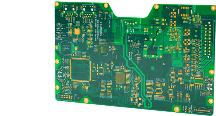
At Fast Turn PCBs, HDI fabrication focuses on accuracy, signal stability, and fast production cycles. Whether it is consumer electronics, telecom equipment, or industrial control systems, HDI boards help engineers achieve compact layouts without sacrificing performance. In this guide, we will explore HDI routing concepts, microvia technology, and manufacturing practices that support ultra-high-density designs.
Understanding HDI PCB Design and Routing Basics
HDI PCB design focuses on fitting more connections into less space while keeping signals clean and stable. This is achieved through fine trace routing, advanced stack-ups, and the use of laser drilled microvia structures. These microvias connect different layers of the board without taking up as much space as traditional through-hole vias, making routing more efficient.
A skilled hdi pcb manufacturer understands how routing decisions affect performance. Proper trace width, spacing, and layer arrangement help reduce noise and improve signal integrity. In modern electronics, even a small routing error can impact speed or reliability, which is why HDI design requires careful planning from the beginning.
Role of Laser Drilled Microvia in HDI Technology
The laser drilled microvia is one of the most important innovations in HDI PCB manufacturing. Unlike mechanical drilling, laser drilling allows extremely small and precise holes that connect only specific layers of the PCB. This supports compact designs and enables high-performance routing in tight spaces.
In collaboration with a reliable hdi pcb manufacturer, engineers use microvias to improve electrical performance and reduce signal path length. Shorter connections mean less delay and lower loss, which is especially important in high-speed digital and RF applications. This technology is essential for smartphones, wearable devices, and advanced computing systems.
HDI Stack-Up Design and Layer Management
A well-planned HDI stack-up is critical for ensuring the board functions correctly. Stack-up refers to how copper layers and dielectric materials are arranged in the PCB. With laser drilled microvia technology, designers can create blind and buried via structures that improve routing flexibility and reduce board size.
An experienced hdi pcb manufacturer carefully controls the stack-up process to maintain impedance consistency and mechanical stability. This is important for high-speed signals, where even small variations in layer thickness can affect performance. Proper stack-up design also helps reduce electromagnetic interference and supports better thermal management.
Signal Integrity and High-Speed Routing Considerations
Signal integrity is one of the biggest challenges in HDI PCB routing. As devices operate at higher frequencies, signals can easily become distorted if routing is not handled properly. Using laser drilled microvia structures helps reduce signal path length, which improves timing and reduces noise.
A professional hdi pcb manufacturer applies strict design rules to maintain controlled impedance and minimize crosstalk. Techniques like via-in-pad design and optimized return paths are often used in HDI layouts. These practices ensure that high-speed signals remain stable and reliable, even in dense circuit environments.
Manufacturing Process of HDI PCBs with Microvias
The manufacturing of HDI boards involves precise steps, starting from material selection to laser drilling and lamination. The laser drilled microvia process requires high accuracy to ensure each via connects the correct layers without damaging surrounding structures. Multiple lamination cycles may be used for complex multilayer designs.
A trusted hdi pcb manufacturer like Fast Turn PCBs uses advanced equipment to maintain tight tolerances during production. Each stage, including imaging, plating, and etching, is carefully controlled to ensure quality. This level of precision is what allows HDI PCBs to perform reliably in demanding applications such as aerospace, automotive, and medical devices.
Applications and Advantages of Ultra HD HDI PCB Technology
Ultra HD HDI PCB technology is widely used in modern electronics that require compact size and high performance. Devices like smartphones, tablets, networking hardware, and IoT systems rely on laser drilled microvia structures to achieve high component density and fast signal transmission. These designs make it possible to integrate more features into smaller products.
Working with an experienced hdi pcb manufacturer ensures that these advantages are fully realized. Benefits include improved electrical performance, reduced board size, and better thermal and mechanical stability. As technology continues to advance, HDI PCBs will remain essential for next-generation electronic systems.
Conclusion
HDI PCB technology continues to shape the future of electronics by enabling smaller, faster, and more powerful devices. Through the use of laser drilled microvia structures and advanced routing methods, designers can achieve high-density layouts without compromising performance or reliability. This makes HDI solutions a core part of modern electronic engineering.
Choosing the right hdi pcb manufacturer is essential for success in HDI design and production. With expert support from Fast Turn PCBs, engineers can develop ultra HD PCB solutions that meet strict performance standards while staying cost-effective and production-ready.
Visit FastTurnPCBs.com for fast, reliable PCB and PCBA manufacturing. From rapid prototypes to full production, we deliver quality circuit solutions to help you bring your electronics to market quickly.